

Founder (and usually tweeting) at @FrameworkPuter
San Francisco, CA
Joined June 2007
- Tweets572
- Following346
- Followers12.8K
- Likes2.9K




Pinned Tweet
Standing offer: If you’re building consumer hardware and want advice on anything (business strategy, building a team, finding suppliers, go to market, design/architecture decisions, fundraising, etc), send me a DM and I am happy to have a call with you.
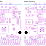
A better example with these instructions from the start. This looks pretty close to what I would have placed and routed by hand (though it is a simple board).


It doesn't take a lot of instruction to make Fable 5.2's routing look closer to what a human would do (though it still loves right angles in traces).


- When placing a PCB, place it the way an experienced layout engineer would by hand:
- For sub-systems sensitive to placements, like ESD protection, crystals, and passives for switching regulators, follow the layout in the relevant datasheet where possible.
- Put each decoupling capacitor directly at the supply pin it serves, with its pad facing the pin and about 1 mm away. Treat a reference design's looser spacing as a maximum, not a target.
- Put every other passive at the pin it serves, oriented so the connection is a short straight trace.
- Group related parts and align them: shared centre lines, even pitch, rows like capacitor – IC – capacitor, test pads on a grid.
- Keep one legible reference label per part, with no overlapping text.
- Review a rendered image of the placement before presenting it, not just DRC, and fix anything that looks scattered or misaligned.
1
6
722
In my CLAUDE.md:
- When routing a PCB, do it the way an experienced layout engineer would by hand:
- No bends sharper than 135°. No square or acute junctions: branch at 45°, and preferably at a pad or via.
- Tracks leave pads and vias from the centre, in a straight run until clear of the copper. No hooks or doubling back.
- Tracks that run the same way within about 0.5 mm of each other are routed side by side at the clearance rule. Plan buses and nets with a common destination as bundles before routing them.
- Leave no gaps that are too narrow to use: either at minimum spacing or wide enough for another track plus clearance. Avoid slivers and pour islands.
- Stagger vias so bundled tracks can stay together up to their ends.
- Start with power pours, then sensitive buses like high speed differential pairs and the micro routing around crystals and switching regulators, then more general bundles of low speed signals.
1
20
774

With DDR and LPDDR shortages and pricing breaking the single board computer category, it's interesting to see that PSRAM-only microcontrollers are getting closer to closing the gap. e.g. ESP32-S31 has a real MMU and can run Linux!

ALT ESP32-S31 mockup in a Raspberry Pi Zero 2 W form factor
Controversial restaurant opinion of the week: Sungho is better than San Ho Won and should have the star instead.
7
1,867
Throwing old projects into Opus 5.5 is fun. It was able to one-shot a solution in 30 minutes to a project I put on hold in 2012: decoding and rendering images from Lytro cameras.
2
11
1,461
My old blog post that the raw image came from: eclecti.cc/computervision/re…
1
649
I just realized, in terms of return on investment, Oculus recently passed AOL-Time Warner as the worst acquisition of all time.


Has anyone ever successfully depleted the battery on a Fluke or Mitutoyo tool? These things might be powered from another dimension.
3
15
1,755
My last post is evenly split between people who think AI can already (or nearly already) route complex boards, and those who think it may never reach human-level. So, how long until AI can competently one-shot a medium-complex 6 layer design that has a few QFNs and BGAs on it?
15%It already can
43%Within the next year
33%Within the next 5 years
10%Never
168 votes • Final resultsBad news. I tried Tony’s Slice House, Pizza Shop, and Arizmendi, and they were all just ok. Is there any New Haven-level pizza in SF?
8
18
4,066
We have much more powerful computers in our portfolio, but a Core Series 3-powered Framework Laptop 12 with Fedora KDE Plasma is my daily driver and the one that brings me the most joy to use.

